
Contents
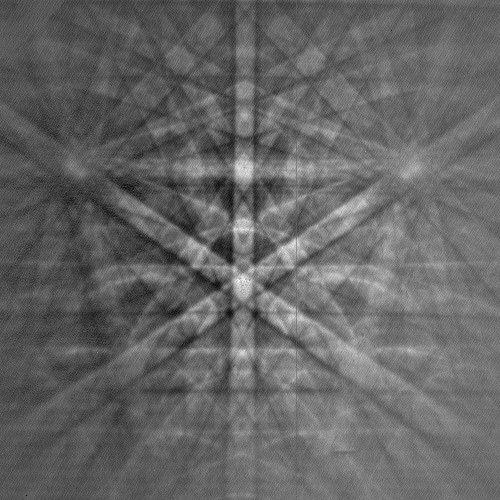
Silicon single crystal at 1024 x 1024 taken
with CCD Fiber Optic Camera (defective optics/electronics)
Back To Top
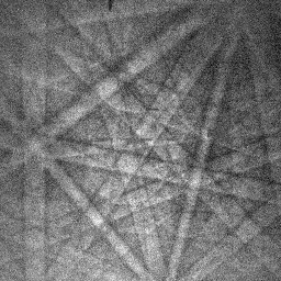
Copper metal at 256 x 256 taken with CCD
Fiber Optic Camera (defective optics/electronics)
Back To Top
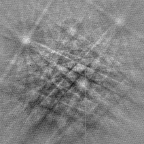
Quatrz at 1024 x 1024 taken with CCD Fiber
Optic Camera (defective optics/electronics)
Back To Top
Back To EPMA Home Page
Back To
Department of Geology and Geophysics Home Page
The Department of Geology and Geophysics
Room 301, McCone Hall
The University of California
Berkeley, CA 94720-4767
Copyright 1998, The Regents of the University of California.